The speed and density of modern electronics is steadily increasing, and while these impressive leaps in technology should allow us to increasingly be able to answer “yes” when asked the question “but does it run Crysis?”, it also means that designers must take greater care when laying out their PCBs – if they want their circuits to be able to run anything at all. This article outlines some of the challenges faced when laying out high-speed digital electronics, and the simulation-techniques used to verify that they have been handled appropriately during the design process, thus ensuring a working product.
The Problem – Time
There are several issues faced during layout of modern high-speed circuits, but for one the digital bandwidth of circuits in the past decades have multiplied manyfold. An increase in digital bandwidth reduces the available setup- and hold time for a signal, i.e. the time before and after the arrival of some clock signal at which some related data signal must remain stable. The consequence of this is that relative arrival times of digital signals within a high-speed interface, routed on a circuit board, must be tightly controlled.

Electromagnetic waves propagate through a circuit board at a rapid pace(a centimetre of typical PCB built from standard dielectrics takes them roughly 60 picoseconds to traverse), but not so fast that it can be ignored when dealing with high-speed digital logic. Some electrical interfaces can account for skew, i.e. timing-mismatches, by introducing internal delays to certain signals in relation to others, but often only to some extent; taking a look at the recommendations given by IC-vendors for propagation-delay matching a DDR5 interface for instance, you might find that they recommend to match bits within a byte to within 50 picoseconds or so – in other words around one centimetre. However, this is not accounting for the fact that before the signals even reach the PCB, they must traverse parts of the processor die and then a bond-wire bonded to the package-pin. This complicates calculations as these internal delays are not equal, (consult the datasheet). In addition, signals routed on interior layers of a PCB propagate faster than those on the outer layers by around a third. Relatedly, since propagation delay is inversely proportional to the square root of the effective dielectric constant of the PCB material, the selected dielectrics must be accounted for as well. What this all means is that one cannot rely on length-matching at all, but must instead match by propagation-delay, which is best handled by tools built into the likes of Cadence Allegro and Altium Designer.
Reflections, Crosstalk and Loss
Fulfilling the given timing relationships are only part of the story; another consequence of the higher data rates is that increasingly shorter PCB-traces must be viewed as transmission lines. In practice, this places demands on the characteristic impedance of a trace. We know that for maximum power-transfer, the impedance of a source should match that of its load. Not doing so results in reflected energy as the trace encounters discontinuities on its path to- or at the load. At slow data rates, this is typically not a signal-integrity problem – energy will bounce back and forth on the line but dissipate before the arrival of the next bit. With sufficiently short periods however, these reflections can blend into future bit periods, giving rise to inter-symbol interference (ISI), in the worst case closing the bit-eye and causing sampling errors. Sources of reflections are many, but include gaps in reference planes, via stubs, incorrect (or missing) termination, and using the wrong trace geometries.
But, as long as propagation delays are matched appropriately, the characteristic impedance as well as the path traversed by a propagating signal carefully considered, all is surely well? Maybe – another consequence (and pre-requisite, really) of higher digital bandwidth is shorter rise- and fall times. Crosstalk, i.e. the phenomenon where a switching trace induces a voltage/current on a neighbouring signal (the “victim”), is directly proportional to the rise- and fall times of the aggressor-line. As electronic circuits decrease in size, the distances between traces become smaller too, and as semiconductor-nodes shrink, the rise- and fall times of IC I/O grow shorter, (owing in part to reduced internal semiconductor parasitics). The consequences of this can sometimes be surprising, as even low-speed signals can cause significant crosstalk owing to the sharp edge-rates of modern I/O. As driving voltages are reduced (many I/O-standards now operate with swings of a few hundred millivolts), this problem is exacerbated.
It is important not to forget about link-budgets either – not all the energy routed into a PCB from a processor- or FPGA I/O will arrive at its destination. Given an otherwise perfect interconnect, some of the signal will be attenuated as it is absorbed by the PCB dielectrics. This phenomenon is frequency dependent, and a measure of it can be found by looking at the dissipation factor or loss tangent given in the dielectric datasheet. For high-speed interfaces, this aspect should not be overlooked.
Signal Integrity Simulations
Many of the pitfalls discussed above can be accounted for by being mindful in the layout process, estimating crosstalk, impedances, and the like as one goes. But to ensure a working interconnect, board-level simulations should be performed, particularly when the speeds are high, the buses wide and the space limited. If one in addition wants to ensure compliance to some standard, it becomes even more important.
There are a few steps to the process:
- First, a PCB layout file is imported into a tool capable of PCB SI simulations, like Ansys SiWave or Keysight ADS.
- A check of the imported stackup, including material properties (e.g., dielectric constants, loss tangents), and copper thicknesses is performed. This is crucial to ensuring that the resulting model reflects real-world behaviour.
- Basic checks like verifying trace-impedances and the like can be performed at this stage, although this is often done beforehand.
- S-parameters of the signal(s) of interest are extracted, derived using the imported layout file and the provided stackup-information.
- These parameters are frequency-dependent and so should be done up to at least some multiple – e.g. to the 5th or 7th – of the fundamental frequency of the digital signal(s) of interest, and with sufficient resolution, i.e. step-size.
At this point one will have a cursory overview of the link quality, since contained in the extracted S-parameters is a measure on insertion- and return loss. In some cases, this is sufficient, but for more thorough simulations, one can go further by using IBIS models in conjunction with the S-parameters.
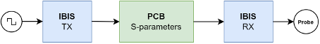
IBIS-models are behavioural models of an I/O, typically provided free-of-charge from the IC-vendor. They model the R, L and C parasitics of a package and a particular I/O pin for some device, as well as its driving characteristics (i.e. the falling- and rising waveforms), diode-clamping behaviour, and internal pullups/pulldowns. An IBIS-model is then connected to its respective port on the extracted S-parameter model in the simulation schematic.
For a full TX/RX-chain, and for a single signal, the resulting setup will look something like the below figure:
To finalise, a few steps remain:
- To produce stimuli, a source is set to drive the transmitting IBIS-model on the TX-side. Its bit-pattern can be chosen arbitrarily, but to cover anumber of different situations (particularly for multi-bit interfaces, since cross-talk is also modelled by the S-parameters), a pseudo-random bit sequence (PRBS) with a different seed for every bit/lane in the simulated signal-group can be used.
- Probes are then placed at points of interest – at least, a probe is placed die-side on the RX-end, instead of at the pin, so that the received signal is measured directly at the receive-circuitry, and not as it appears exterior to the device-pin, where it is not yet affected by the device parasitics.
- Finally, a simulation is set up with a duration sufficient to cover a substantial number of permutations of the bit pattern driven at each period.
The simulation results can then be used to construct one or more eye-diagrams, i.e. a superposition of several bits sampled at the receiving end, with sampling triggered by a clock or some other timing reference. From this, jitter, high/low-voltages, rise-and-fall times as well as bit-error-rates for the physical link can be estimated, and pass/fail-criteria can be embedded to verify compliance to some standard. Shown below is an example of such an eye-diagram, for a single bit belonging to an LPDDR4X interface running at 3733Mb/s
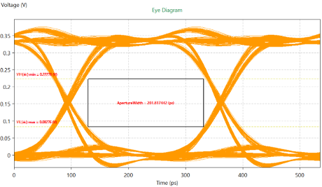
If the right considerations have been taken during the layout process, ideally a clean, open eye is seen, and otherwise, the layout can be revised. It probably does not need to be said that this is preferable to spending time and money on revised physical PCBs after the first batch was found to be non-functional.